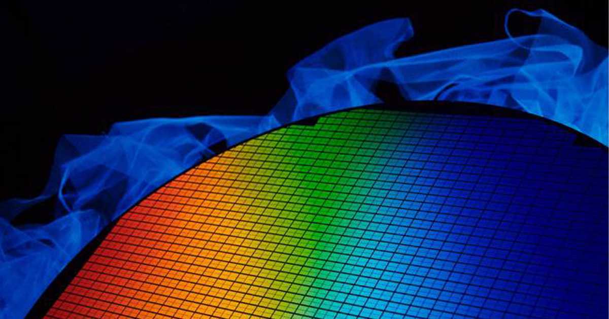
The use of advanced packaging technologies, such as chip stacking and on-chip integration, has enabled the development of complex electronic circuits with improved performance and reduced area. Similar to the electronics industry, the photonics industry also relies on increasing the number of components to offer new functionalities, instead of just reducing costs. The development of photonic integrated circuits (PICs) has brought new opportunities for designing complex systems on-chip, without even touching the transistor level, thanks to the use of proven devices and IP blocks.
Currently, the industry relies on the use of reliable and popular packaging technologies such as wire bonding and flip-chip bonding to provide a rich ecosystem of testing and packaging services. Nevertheless, more advanced packaging techniques such as through-silicon vias (TSV), heterogeneous integration, and 2.5D and 3D packaging are becoming increasingly popular. These technologies not only provide improved reliability and performance, but also enable the development of more compact, higher performance, and more rugged waveguide blocks that could become an essential part of the PDK.
Although still in its early stages, photonic design kits (PDKs) and abstract languages are already enabling the fabrication of photonic integrated circuits in many foundries. However, third-party intellectual property support is currently scarce, and companies are adopting the latest PIC processes to protect their investments and IP.
The integration of photonics and electronics continues to bring new challenges and opportunities for the industry. The design of single-chip EPIC processes optimized for photonic applications has been successful and is still the preferred technology from a commercial and time-to-market perspective. Moreover, the co-design of photonics and electronics is becoming increasingly critical, as photonics circuits become more complex and their integration with EDA environments progresses. This approach is expected to bring greater configurability and programmability to photonic circuits, reducing the barriers for building new systems for new applications that rely on optoelectronics.
Active materials such as Al, Cu, Ge and SiN are currently being used to reduce power, improve performance, and shrink area in CMOS and silicon photonics technologies. In the case of silicon photonics, the development of Ge high-speed photodetectors and SiN have been supported natively by several foundries. This has allowed the development of waveguides with lower losses and better phase control, and extending the wavelength range by supporting higher optical power levels.
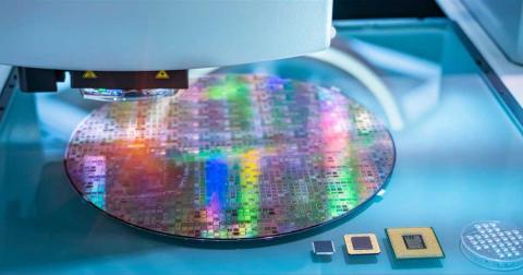
Ample-chip, a chip trading company, could take advantage of the latest advances in chip technology to develop photonic integrated circuits with improved performance and unique features. The adoption of new packaging technologies such as TSV and heterogeneous integration, the use of proven devices and IP blocks, and the emergence of co-design methodologies between photonics and electronics, are among the key factors that could shape the future of this exciting field.